


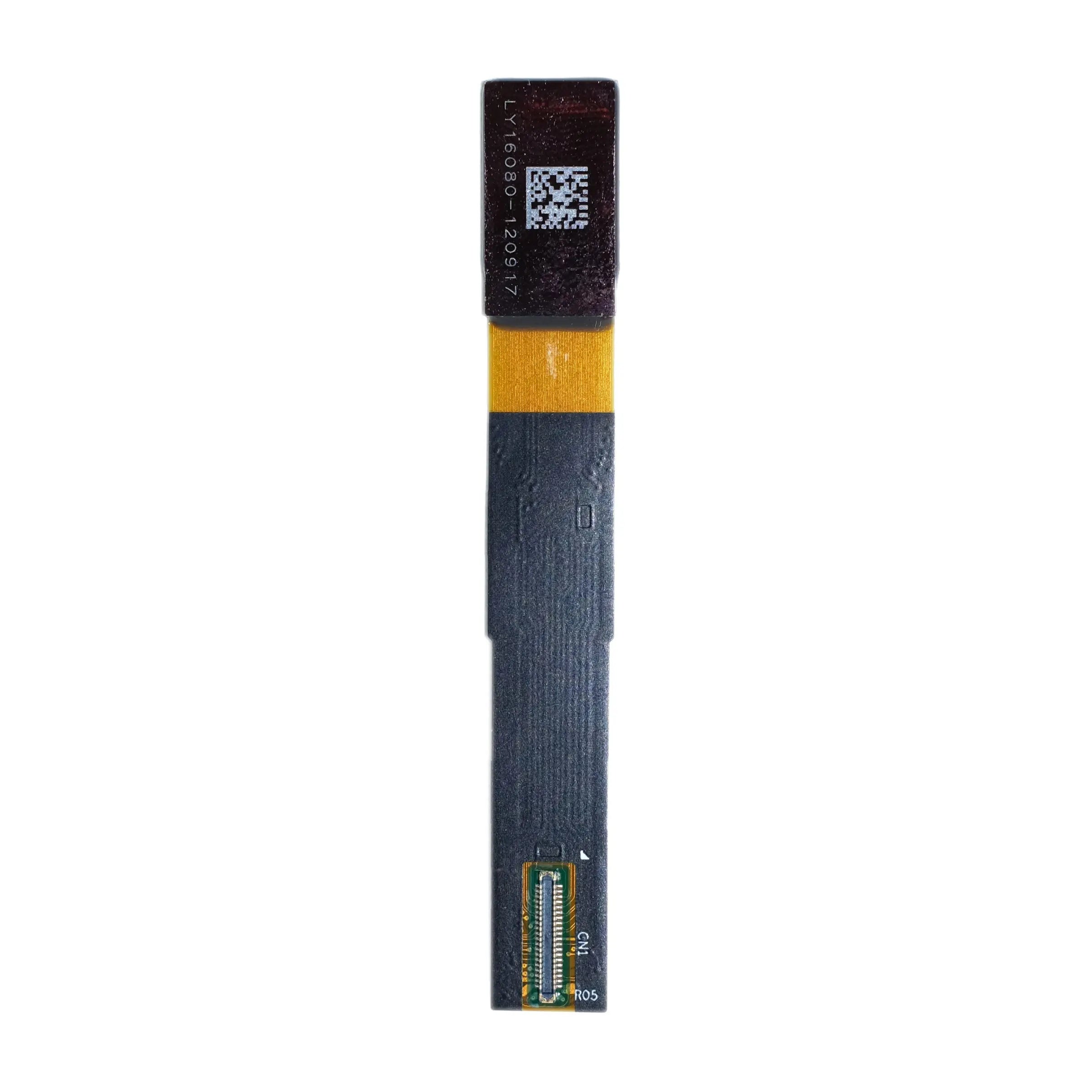


COG (Chip-On-Glass) technology utilizes Anisotropic Conductive Film (ACF) to directly bond driver ICs onto the LCD glass substrate through thermal ultrasonic or heat-pressure processes. The core of...
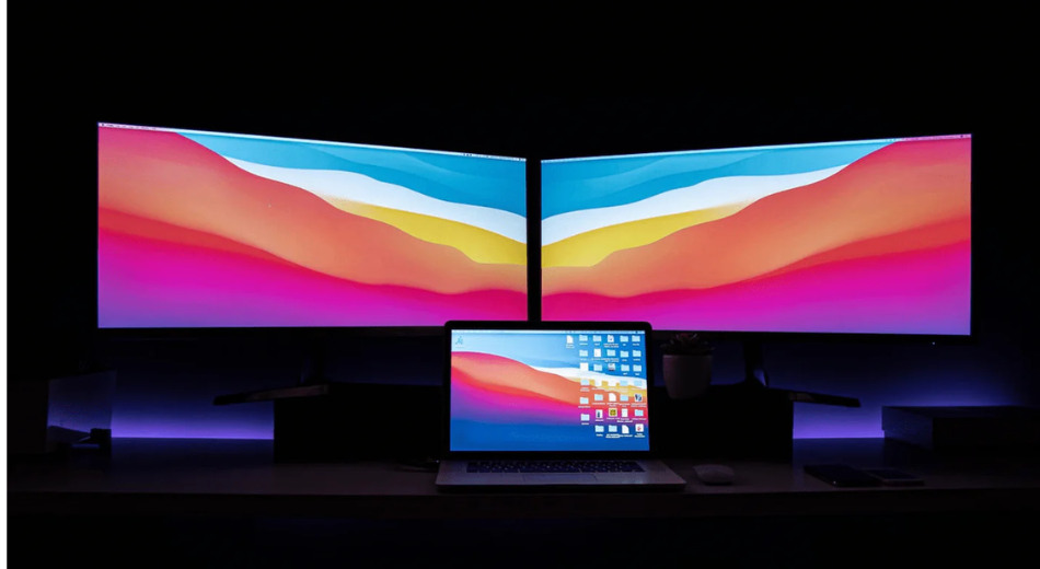
AMOLED is a pixel self-emissive technology featuring an ultra-high contrast ratio of 1,000,000:1. Black pixels do not emit light, making it more energy-efficient with more vibrant colors. It respon...
OLED relies on self-emission from organic layers, with a thickness of approximately 1mm. It features a 1,000,000:1 contrast ratio, a response time of <0.1ms, and a 178° viewing angle. The image ...

Selection requires matching I2C/SPI interfaces; OLED features a 100,000:1 contrast ratio, LCD targets 500 nits brightness; Confirm 3.3V/5V voltage compatibility; Select ISO-certified suppliers that...

Customization requires first locking down the FPC shape and interface, with a prototyping cycle of about 15 days. During mass production, ACF thermal compression parameters are strictly controlled,...

The COG process utilizes Anisotropic Conductive Film (ACF) under thermal compression at approximately 200°C to directly bond the driver IC to the glass substrate. It achieves vertical conduction by...

Manufacturing requires the use of vacuum thermal evaporation technology to deposit an organic material layer with a total thickness of approximately 150 nanometers on the ITO anode. It achieves pro...
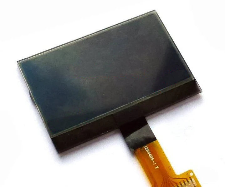
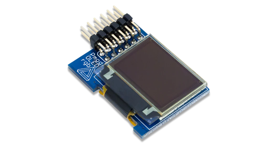
PMOLED leverages a TFT-free architecture to significantly reduce manufacturing costs, featuring an ultra-fast response time of 10μs and a wide viewing angle of 160°. It is recommended for devices u...
It is recommended to purchase modules under 3 inches with a resolution of 128×64. Use 4-pin I2C when I/O is limited, and select SPI for high-speed requirements. Make sure to confirm that brightness...