


How OLEDs Work? - OLED Structure & Principle of Luminescence
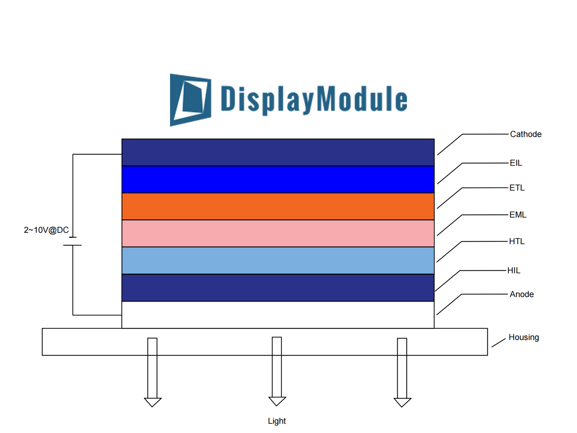
OLEDs emit light via organic films (100–200nm thick) sandwiched between anode/cathode. Electrons/holes inject, merge in emissive layer, exciting molecules to release photons (100% NTSC color). No backlight: self-luminous, enabling thin/flexible screens like LG’s rollable TVs.
The Basic OLED Sandwich Layers
Imagine a multi-layered sandwich, but one where each layer is thinner than a single human hair, with a total thickness often measuring less than 500 nanometers. This entire stack is built on a substrate, which can be rigid glass or flexible plastic foil as thin as 0.2 millimeters. The fundamental innovation lies in replacing the bulky, power-hungry backlight required by LCDs with these thin organic films that emit their own light. A key driver for this technology's adoption is cost; manufacturing an OLED panel is estimated to be 30-40% cheaper than a comparable TFT-LCD because it requires fewer overall layers and materials.The bottom anode is typically made of a transparent conductor like Indium Tin Oxide (ITO), which has a high work function of around 4.7 eV to facilitate the injection of positive charges. The top cathode, often a blend of magnesium and silver (Mg:Ag) or a similar alloy, has a low work function, typically below 4.0 eV, optimized for injecting electrons.
The thickness of each of these organic layers is critically controlled, usually within a range of 50 to 200 nanometers. For example, a common HTL material like NPB might be deposited to a thickness of 60 nm, while the EML itself could be a mere 30 nm thick. Without it, charges can get trapped, generating heat instead of light and reducing the device's operational lifespan, which can range from 10,000 to over 50,000 hours to half brightness, depending on the materials and driving conditions.
The function of the layered design is to force charge carriers—holes and electrons—to meet in a specific zone: the Emissive Layer (EML). This controlled meeting is what enables efficient light generation.
The following table outlines the typical materials and their key characteristics in a standard OLED stack:
|
Layer |
Common Material(s) |
Typical Thickness |
Primary Function |
Key Parameter (Work Function / Energy Level) |
|---|---|---|---|---|
| Anode | ITO (Indium Tin Oxide) | 100-150 nm | Inject holes (positive charges) | High Work Function (~4.7 eV) |
| Hole Transport Layer (HTL) | NPB, TPD | 40-60 nm | Transport holes to the EML | HOMO Level: ~5.1 - 5.4 eV |
| Emissive Layer (EML) | Alq3, host-dopant systems | 20-40 nm | Region for light emission | Bandgap determines light color |
| Electron Transport Layer (ETL) | Alq3, TPBi | 40-60 nm | Transport electrons to the EML | LUMO Level: ~2.7 - 3.0 eV |
| Cathode | Mg:Ag alloy, LiF/Al | 100-200 nm | Inject electrons (negative charges) | Low Work Function (< 4.0 eV) |
When a low DC voltage, typically between 2 and 10 volts, is applied across the electrodes, electrical current flows. Holes injected from the ITO anode move through the HTL, while electrons from the metal cathode move through the ETL. The entire process, from charge injection to light emission, happens incredibly fast, with a response time of less than 10 microseconds (µs), which is about 1,000 times faster than a standard LCD pixel.
Understanding the Emissive Layer
The Emissive Layer (EML) is the literal and figurative light source of an OLED, the 20 to 40 nanometer-thin heart where electrical energy is directly converted into visible photons. This conversion process, known as electrophosphorescence, is remarkably efficient. Unlike LCDs that rely on a static backlight and color filters that block over 70% of the initial light, the EML creates light on demand. This fundamental difference is a primary reason OLED displays can achieve perfect blacks and a theoretically infinite contrast ratio, as each pixel can be completely turned off. The specific color of light emitted—whether a deep red with a wavelength of 620 nanometers or a pure green at 530 nanometers—is determined by the precise chemical structure of the organic molecules within the EML.
Statistically, the electrical charge injection results in the formation of singlet and triplet excitons in a ratio of 1:3. This means that only 25% of the excitons are singlets (which can decay to emit light via fluorescence) while a majority 75% are triplets, which would typically be lost as heat in early OLED materials. The development of phosphorescent materials was a breakthrough, as they can harness the energy from both singlet and triplet excitons, boosting the internal quantum efficiency potential from 25% to nearly 100%. The actual external quantum efficiency (EQE) of a commercial OLED device, which accounts for light extraction challenges, typically ranges from 5% to over 20% for the most advanced units. The intensity of the light output is directly proportional to the current density; for a typical smartphone OLED pixel, a current density of about 10 mA/cm² might produce a brightness of over 300 candelas per square meter (cd/m²), which is suitable for indoor viewing.
A host matrix, making up about 90-95% of the layer by volume, is responsible for managing the transport and energy transfer. A guest dopant molecule, at a carefully controlled concentration often between 5% and 10%, is where the actual light emission occurs. This doping process is critical for stabilizing the material and shifting the emission color. For example, a red dopant like Ir(mpq)₂(acac) in a host matrix like CBP will emit light with a peak wavelength of about 610 nm and a full-width at half-maximum (FWHM) of roughly 70 nm, which defines the color purity. The following table contrasts the key characteristics of emissive materials for the primary colors:
|
Material Type / Color |
Common Example(s) |
Peak Wavelength (nm) |
External Quantum Efficiency (EQE, max %) |
Relative Operational Lifetime (T50 @ 1000 nits) |
|---|---|---|---|---|
| Fluorescent (Blue) | DPVBi | ~450 - 460 | ~5 - 6% | 1x (Reference, ~10,000 hours) |
| Phosphorescent (Green) | Ir(ppy)₃ | ~510 - 530 | ~20 - 30% | > 10x longer than Fluorescent Blue |
| Phosphorescent (Red) | Ir(mpq)₂(acac) | ~610 - 620 | ~20 - 25% | > 20x longer than Fluorescent Blue |
The precise energy levels of the EML materials are paramount. The host material must have a slightly wider bandgap than the dopant to ensure that the exciton's energy is cleanly transferred to and confined on the guest molecule. This energy transfer happens with an efficiency exceeding 90% in well-designed systems. The drive voltage for light emission is low, typically between 2.5 and 4 volts to initiate visible light, scaling up to 8-10 volts for high brightness levels exceeding 1,000 cd/m². The response time of this entire process, from carrier injection to photon emission, is exceptionally fast, occurring in less than 10 microseconds (μs), which is about 1,000 times faster than the response time of a standard LCD pixel.

How Electricity Creates Light
The transformation of electricity into light within an OLED is a remarkably direct and efficient process that occurs on a molecular scale in less than 10 microseconds (μs). When a low DC voltage, typically between 2 and 10 volts, is applied across the device's electrodes, it creates an electric field with a strength of approximately 10^6 to 10^7 volts per meter across the organic layers. This field provides the driving force for charge carriers.
From the anode (commonly ITO with a work function of ~4.7 eV), positive charges or "holes" are injected into the organic stack. Simultaneously, from the cathode (often a Mg:Ag alloy with a work function below 4.0 eV), electrons are injected. The current density required for standard smartphone display brightness of around 300 cd/m² is relatively low, roughly 10 mA/cm². This direct electrical excitation is fundamentally different from LCD technology, where the LED backlight alone can consume over 50% of the panel's total power budget, much of which is then filtered out.
Holes travel through the Hole Transport Layer (HTL), which has a Highest Occupied Molecular Orbital (HOMO) level around 5.2 eV, while electrons move through the Electron Transport Layer (ETL) with a Lowest Unoccupied Molecular Orbital (LUMO) level near 2.8 eV. The energy level alignment is critical; a mismatch greater than 0.3 eV can create a significant barrier, reducing efficiency by over 20% and generating wasteful heat. The primary destination for both charge types is the Emissive Layer (EML), a zone only 20-40 nanometers thick. The probability of an electron and a hole meeting in this layer is high due to the confined space.
When they meet, they are bound together by Coulombic attraction with a force of approximately 8 x 10^{-8} Newtons, forming a quasi-particle called an exciton. Statistically, this process generates 25% singlet excitons and 75% triplet excitons. The use of phosphorescent materials is crucial here, as it allows the device to harness the energy from both types of excitons, boosting the theoretical internal quantum efficiency from a maximum of 25% for fluorescent materials to nearly 100%.
Building a Simple OLED Device
The journey begins with a substrate, typically a 0.7 mm thick glass pane coated with a 150 nm layer of Indium Tin Oxide (ITO) which serves as the transparent anode. The ITO's sheet resistance is a critical parameter, usually between 10 and 20 ohms per square, as higher resistance can lead to voltage drops across the display. The substrate undergoes a rigorous cleaning process involving ultrasonic baths with solvents like acetone and isopropyl alcohol, each cycle lasting 10 to 15 minutes, to remove microscopic contaminants that could cause electrical shorts.
The entire fabrication process must be carried out in a Class 1000 or better cleanroom environment, where the number of dust particles larger than 0.5 micrometers is limited to less than 1000 per cubic meter. The core of the process is the sequential deposition of the organic layers, which must be accomplished without exposing the sensitive materials to oxygen or moisture, as even 1 part per million (ppm) of these can reduce the device's operational lifetime by over 50%.
The base pressure inside the chamber must be extremely low, on the order of 1 x 10^-6 Pascals or better, to ensure a mean free path long enough for the organic molecules to travel in a straight line from the heated source to the substrate. The substrate is usually held at a distance of 30 to 50 centimeters from the evaporation sources. Each organic material is heated in a separate, temperature-controlled ceramic crucible. The evaporation rate for each material is precisely controlled, often between 1 and 5 Angstroms per second (0.1 to 0.5 nm/s), and monitored in real-time using a quartz crystal microbalance.
The Hole Transport Layer (HTL) might be deposited to a thickness of 60 nm, the Emissive Layer (EML) to 30 nm, and the Electron Transport Layer (ETL) to 40 nm, with a thickness uniformity tolerance of better than ±5% across the substrate.Following the organic layers, the cathode, often a 100 nm thick layer of a Magnesium-Silver (Mg:Ag) alloy in a 10:1 ratio, is evaporated through a shadow mask to define the individual pixel areas. The entire multi-layer stack is built without breaking vacuum, a process that can take 45 to 90 minutes for a single substrate.
Creating Colors with OLEDs
Unlike LCDs that rely on a white LED backlight and color filters that block over 70% of the light, resulting in a typical power efficiency of only 3-5 lumens per watt, OLEDs create pure colors on demand. The specific color emitted is determined by the bandgap energy of the organic molecules in the emissive layer (EML). A larger bandgap results in higher-energy, shorter-wavelength light, such as blue, with a wavelength of around 450-460 nanometers, while a smaller bandgap produces lower-energy, longer-wavelength light, like red, at 620-640 nanometers. The purity of the color is measured by its Full Width at Half Maximum (FWHM), which for a typical OLED emitter is a relatively narrow 30-50 nm, leading to highly saturated colors. This allows OLED displays to achieve a wide color gamut, often covering 100% or more of the DCI-P3 color space, which is about 25% wider than the standard sRGB gamut used in many LCDs. The key challenge lies in developing stable and efficient emitters for all three primary colors, particularly blue, where the high-energy photons accelerate material degradation, limiting the operational lifetime to approximately 15,000 hours to half-brightness, compared to over 50,000 hours for some red and green phosphorescent emitters.
There are several primary methods used to create the full spectrum of colors in OLED displays, each with distinct advantages and trade-offs in terms of manufacturing cost, efficiency, and color purity.
-
Side-by-Side Patterning (RGB): This method deposits individual red, green, and blue emissive materials directly onto the substrate through a fine metal mask (FMM). Each pixel is composed of three distinct sub-pixels. The challenge is patterning the tiny sub-pixels, especially for high-resolution displays above 400 pixels per inch (PPI), which requires a FMM with slit widths of less than 20 micrometers. This method offers the best color gamut, often exceeding 110% of the NTSC standard, but can have higher manufacturing costs and potential color balance issues over the display's lifespan due to the different aging rates of the materials.
-
White OLED with Color Filters (WOLED-CF): Here, a single, broadband white-light OLED stack is used. This white light is then passed through sophisticated red, green, and blue color filters, similar to an LCD, to create the colors. The white OLED emitter typically has a power efficiency of 10-15 lumens per watt. While this approach is more manufacturable for large screens and avoids color imbalance, the color filters absorb a significant amount of light, reducing the overall efficiency by about 60-70%. This method often results in a slightly smaller color gamut, around 90-100% of the DCI-P3 space.
-
Blue OLED with Color Conversion (QLED): A emerging hybrid approach uses a highly efficient and stable blue OLED as the primary light source. This blue light then excites quantum dot (QD) color conversion layers. The quantum dots, which are nanocrystals with a diameter of 2-10 nanometers, absorb the blue light and re-emit it as very pure red or green light with a FWHM of just 20-35 nm. This method can achieve the widest color gamut, potentially exceeding 140% of the DCI-P3 standard, with high power efficiency because the color conversion process is more efficient than filtration.
Fluorescent materials, historically used for blue light, have a maximum internal quantum efficiency (IQE) limit of 25% because they can only utilize singlet excitons. Phosphorescent materials, which are standard for red and green, can harness both singlet and triplet excitons, achieving an IQE of nearly 100%. A third type, Thermally Activated Delayed Fluorescence (TADF) emitters, are in development to achieve 100% IQE without using expensive rare-earth metals like Iridium, potentially reducing material costs by 20-30%. The driving current also influences color; a 50% increase in current density might boost brightness by 50% but can cause a slight wavelength shift of 1-3 nm, which must be calibrated electronically. The pursuit of perfect color in OLEDs is a balance of chemistry, physics, and engineering, aiming to maximize both the visual experience—with color gamuts targeting Rec. 2020 standards—and the product's longevity, ensuring consistent color output for over 10,000 hours of use.
Real-World OLED Screen Designs
A common high-end smartphone display, with a 6.1-inch diagonal and a resolution of 2532 x 1170 pixels, packs over 3 million individual pixels, resulting in a pixel density of about 460 PPI (Pixels Per Inch). The average thickness of this entire display assembly can be as low as 1.5 mm, a 60% reduction compared to a typical LCD module. Power consumption varies significantly with content; displaying a black image may use less than 0.5 watts, while a full-white screen at high brightness could draw 3-4 watts.
|
Product Category |
Typical Size & Resolution |
Key OLED Design Feature |
Average Thickness |
Peak Brightness (HDR) |
Approx. Power Consumption |
|---|---|---|---|---|---|
| Smartphone | 6.1-inch, 2532x1170 (~460 PPI) | Rigid or Flexible substrate, On-cell touch | 1.5 - 2.0 mm | 1200 - 2000 nits | 1 - 4 W (variable) |
| Television | 55-inch, 3840x2160 (~80 PPI) | White OLED (WOLED) with Color Filter | 4 - 5 mm (panel only) | 800 - 1000 nits | 50 - 150 W (variable) |
| Smartwatch | 1.5-inch, 360x360 (~300 PPI) | Flexible Plastic Substrate, Low Refresh Rate | < 1.0 mm (with touch) | 800 - 1200 nits | 0.2 - 0.8 W |
In practice, manufacturers use different design approaches to balance performance, cost, and manufacturability. The two most prevalent designs are:
-
RGB Side-by-Side: This method uses Fine Metal Masks (FMM) to vapor-deposit individual red, green, and blue organic materials directly onto the TFT backplane to form subpixels. The mask for a 6.1-inch 460 PPI display has openings with a tolerance of less than 5 micrometers. This design offers the widest color gamut, often 110% of the DCI-P3 standard, but can suffer from color imbalance over a 10,000-hour lifespan due to different material degradation rates.
-
White OLED with Color Filters (WOLED-CF): Used primarily in large-area televisions, this design employs a stack that emits white light. This white light is then passed through red, green, and blue color filters to create the subpixels. While this avoids the intricate patterning of RGB and improves manufacturing yield by approximately 15%, the color filters block about 65% of the generated light, reducing overall power efficiency to around 5-8 lumens per watt.
The drive transistor must supply a consistent current to the OLED to maintain stable brightness; even a 5% variance in current can lead to visible non-uniformity. For flexible displays, the rigid glass substrate is replaced with a polyimide (PI) film, typically 10-20 micrometers thick, which is coated directly onto a carrier glass. After the TFT and OLED layers are built, the glass is laser-lifted, leaving a flexible screen that can withstand over 200,000 bending cycles to a radius of 3 mm. A significant design challenge is managing the different aging rates of the colored pixels. Blue pixels degrade fastest, with a luminance half-life of about 15,000 hours at a standard brightness of 200 nits, compared to over 50,000 hours for red and green. To combat this, screen designs incorporate sophisticated compensation algorithms that run 60 times per second to adjust the voltage supplied to each pixel, counteracting the gradual efficiency drop and preventing "burn-in". Modern designs also integrate touch sensors directly into the display structure (on-cell or in-cell touch), reducing thickness by another 0.3 mm compared to using a separate touch layer.
Read more
LCD means Liquid Crystal Display, using liquid crystals sandwiched between polarized glass to modulate backlight, creating images. Common in TVs/phones, IPS panels (e.g., iPad Pro) offer 178° viewi...
TFT structures comprise a glass substrate, gate electrode (Mo, 100–200nm thick), SiO₂ insulator (≈300nm), semiconductor layer (a-Si, 50–100nm), and source/drain metals (150–200nm). Gate volta...
Leave a comment
This site is protected by hCaptcha and the hCaptcha Privacy Policy and Terms of Service apply.